


While the pixels shown in Figure 1 appear to be square and to "cover" the continuous image, it is important to know the geometry for a given camera/digitizer system. In Figure 18 we define possible parameters associated with a camera and digitizer and the effect they have upon the pixel.
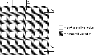
Figure 18: Pixel form parameters
The parameters Xo and Yo are the spacing between the pixel centers and represent the sampling distances from equation . The parameters Xa and Ya are the dimensions of that portion of the camera's surface that is sensitive to light. As mentioned in Section 2.3, different video digitizers (frame grabbers) can have different values for Xo while they have a common value for Yo.

Figure 19: Effect of non-square pixels
The ratio Xo / Yo can be determined for any specific camera/digitizer system by using a calibration test chart with known distances in the horizontal and vertical direction. These are straightforward to make with modern laser printers. The test chart can then be scanned and the sampling distances Xo and Yo determined.
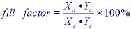
The larger the fill factor the more light will be captured by the chip up to the maximum of 100%. This helps improve the SNR. As a tradeoff, however, larger values of the fill factor mean more spatial smoothing due to the aperture effect described in Section 5.1.1. This is illustrated in Figure 16.